Effect: Diffusion
During the propagation of electrons inside the silicon, they are repeatedly scattered that leads to their displacement in the pixel plane.
Contact person(s) if any:
Craig Lage, Andrei Nomerotski/SAWG
Reference Material:
Description of theoretical model used to estimate electron diffusion amplitude is given in Craig Lage’ document on Poisson_CCD22 low-level simulator. Discussion of whether this model properly describes the diffusion of Fe66 hits seen in the experiments is presented in the following talks by Sergey Karpov - 1, 2 and by Craig Lage - 3.
Also some information, including previous efforts of measuring voltage dependency of diffusion, is available in the Andy Rasmussen article 4
Data Provenance:
Data for validation are taken from the following sensors tested at BNL under different bias voltages:
ITL-3800C-092
ITL-3800C-095
ITL-3800C-307
E2V-CCD250-107
Model Details:
The amount of diffusion to apply was defined in GalSim:galsim/sensor.py, inside _calculate_diff_step function. Before Aug 8, 2018, it was defined as
# 0.026 is kT/q at room temp (298 K)
diff_step = np.sqrt(2 * 0.026 * CCDTemperature / 298.0 / Vdiff) * SensorThickness
It implemented the diffusion model explained in detail in Appendix E of this document.
This model is known to underestimate the diffusion by ~2 times in respect to experimental data on Fe55 hits, so the use of an effective electron mass correction from Green (1989) has been proposed by Craig Lage.
Since Aug 8, it is implemented as:
# Set up the diffusion step size at the operating temperature
# First, calculate the approximate front side voltage
VChannelStop = qfh # near zero
VCollect = Vparallel_hi + 12.0 # Estimate from simulation
VBarrier = Vparallel_lo + 15.0 # Estimate from simulation
ChannelStopRegionWidth = 2.0 * (ChannelStopWidth / 2.0 + FieldOxideTaper)
ChannelStopRegionArea = ChannelStopRegionWidth * PixelSize
CollectArea = (PixelSize - ChannelStopRegionWidth) * PixelSize * CollectingPhases / NumPhases
BarrierArea = (PixelSize - ChannelStopRegionWidth) * PixelSize * (NumPhases - CollectingPhases) / NumPhases
Vfront = (ChannelStopRegionArea * VChannelStop + CollectArea * VCollect + BarrierArea * VBarrier) / (PixelSize**2)
# Then, the total voltage across the silicon
Vdiff = max(Vfront - Vbb, 1.0) # This just makes sure that Vdiff is always > 1.0V
MobilityFactor = 0.27 # This is the factor from Green et.al.
# 0.026 is kT/q at room temp (298 K)
diff_step = np.sqrt(2 * 0.026 * CCDTemperature / 298.0 / Vdiff / MobilityFactor) * SensorThickness
This implements both the effective mass correction (through MobilityFactor multiplier), and the adjustments for Vfront front voltage based on simulations using the peak voltage at ~1 um above the bottom.
The diff_step value computed above describes the diffusion for
outer surface electron conversion. If the electron is generated at
some depth inside the silicon, the value is scaled down as
diffusion = diff_step * sqrt(1 - ConversionDepth/SensorThickness)
This is done inside Silicon::accumulate() method of GalSim Silicon.cpp.
Validation Criteria:
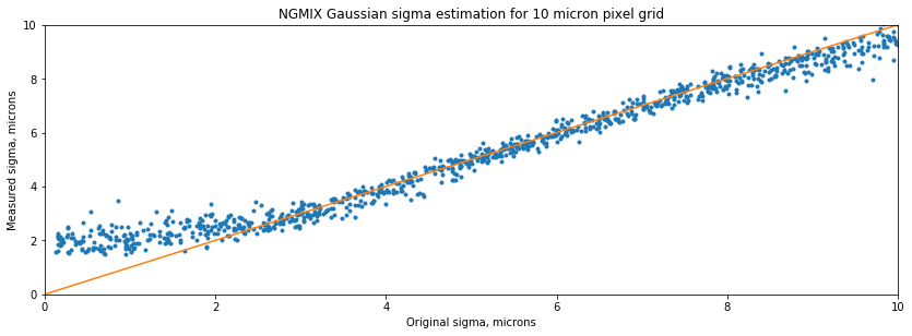
The amount of diffusion under different experimental setups is measured by fitting the Fe55 hit marks in acquired images with Gaussian model using NGMIX code by Erin Sheldon. The validity of fitting procedure for significantly undersampled case of Fe55 hits has been specifically studied by generating and pixelizing the clouds of electrons with different sizes and sub-pixel center positions, fitting them in the same way as Fe55 hits, and then comparing the results with original sizes. The procedure has been found to be unbiased in the parameter region of interest for Fe55 fitting, and therefore applicable for the validation.

Validation of NGMIX Gaussian fitter
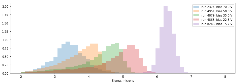
The following distributions have been obtained for the sizes of Fe55 hits (selecting only the events corresponding to main Kalpha intensity peak) under different bias voltages on different CCDs:

Sizes of Fe55 hits under different voltages
The following table summarizes these distributions in terms of median (which corresponds to the ~28 um mean conversion depth of Fe55 x-ray photons in silicon) and surface conversion diffusion values:
Voltage, V |
Run Number |
Sensor |
Median diffusion, um |
Surface conversion diffusion, um |
|---|---|---|---|---|
15.7 |
8246 |
ITL-3800C-307 |
6.3 |
6.66 |
22.2 |
4863 |
ITL-3800C-092 |
4.95 |
5.47 |
35 |
4879 |
ITL-3800C-092 |
4.48 |
4.95 |
50 |
4951 |
ITL-3800C-095 |
3.83 |
4.27 |
70 |
2374 |
E2V-CCD250-107 |
3.41 |
3.85 |
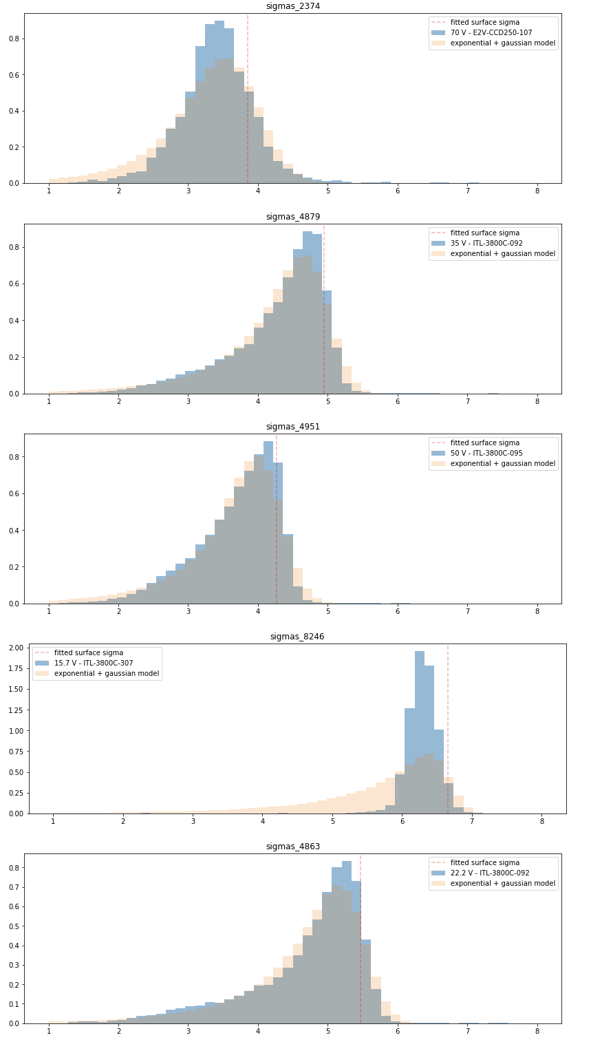
The latter is derived from fitting the distributions with the model consisting of exponentially distributed conversion depth and gaussian scatter of measured sigmas. Details of the fits are shown here

Fit of the distributions of the sizes of Fe55 hits with the model consisting of exponentially distributed conversion depth and gaussian scatter of measured sigmas.
Lowest and highest voltages fits are probably not completely reliable as the histograms deviate from expected shape. All other voltages are described quite well by such simple model.
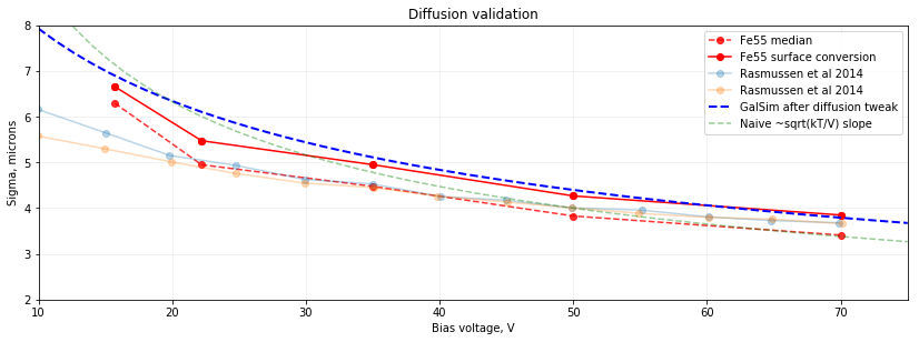
Moreover, the data on surface conversion diffusion acquired earlier and published in Rasmussen et al (2014) are also used for qualitative validation.
Validation Results:
Since Aug 8, 2018 GalSim uses the diffusion model that is mostly consistent with the Fe55 results shown above.

Comparison of the GalSim diffusion amplitude with the sizes of Fe55 hits for different bias voltages
Small discrepancy is seen for lower voltages and is most probably
related to unoptimal Vfront adjustment.
Relevant Project Team for input if any:
Camera
Release and approval log:
07/20/18 - Initial Version - Sergey Karpov
08/08/18 - Update for a new diffusion model committed by Craig Lage - Sergey Karpov